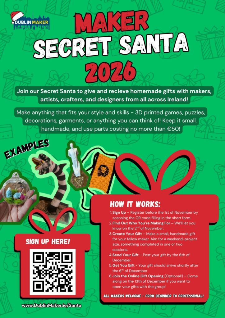
Dublin Maker’s Maker Secret Santa is back, and it’s a good excuse to make something for another maker this Christmas.
Lots of TOG members have taken part over the years. Making a gift for someone you might never have met is an interesting challenge, and there’s the fun of finding out what someone else has made for you.
Previous exchanges have included Jeffrey’s keypad memory game and Nathan’s miniature Crumlin Shopping Centre. You can read about both in our earlier blog post. We would recommend starting a little earlier than Jeffrey did. He finished his build and locked up the hackerspace at 2 am!
The idea is simple: sign up, get matched with another maker, make them a small gift and post it off. Everyone can then join an online gift opening to see what people have made.
It’s open to makers across the island of Ireland, at all levels of experience. You don’t need to have taken part in Dublin Maker before. Whether you’re into electronics, knitting, 3D printing, painting or something else, there’s room for your way of making.
Dublin Maker recommends choosing a project you can finish in one or two making sessions and spending no more than €50 on parts and materials. Using what you already have is a good place to start.
The dates for 2026 are:
- 1 November: Sign-up deadline.
- 2 November: Find out who you’re making for.
- 6 December: Post your gift by this date.
- 13 December: Join the online gift opening.
Fancy taking part? Find the full details and sign up on the Dublin Maker website.